… or a story about how I suck at choosing the proper file
The story
Once upon a time, there was a little pony called Bungholio …

OK! OK! Wrong story. Let me start it over again.
Fried 8580
It all started as a fun project. My fellow group member Johny of Lamers asked me if I could make a hardware replacement for his fried SID 8580. He sent me a link to a website with an awesome project – SwinSID – It was created by Swinkels (Cheers mate!).
http://www.swinkels.tvtom.pl/swinsid/
Challenge accepted!
Homemade PCBs
I’ve started with one of the early versions of SwinSID, more precisely SwinSID SE.
I chose it because it required easy-to-solder THT components and
it had a simplified, one-sided version of PCB.
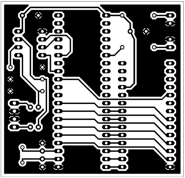
It was supposed to be a totally homemade project so I’ve decided to go with the toner-transfer method …. like in the ’90s 😀
First, a step required printing layout in a proper size on a paper coated with a mysterious substance.
protip time: This special paper can be found in nearly all homes nowadays, most probably near a toilet throne, so the king can read while “ruling” his kingdom lol. It is simply a paper from color magazines – the thinner, the better. All you have to do is to cut a few pages out and print on it a PCB board layout with a Laser printer.
Next, you have two options. Either go with iron like in the ’90s …. or buy a cheap laminator and hack it to suit your needs. In my case, it was, of course, a laminator. The hack relied on removing overheating protection and changing a few resistors so a laminator could run at higher temperatures. Also cutting out unnecessary parts of the plastic case might be handy for larger PCBs
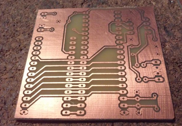
Etching
Now armed with a “pro” tool, I could proceed with toner transfer by simply pushing a blank PCB with a taped-on printout into the laminator (HINT: use Kapton tape). Just a few passes are needed to transfer toner to PCB. Then I put it into the jar filled with water and after a few minutes, I was able to slowly tear off the soaked paper. I was ready to etch my PCB. For etching I use Sodium Persulfate – works like a charm.
Here is a result.
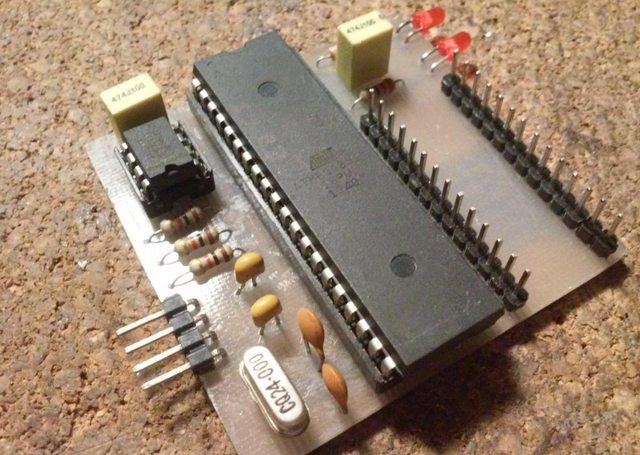
Finally, I could solder on some parts.
Here is a photo of nearly complete PCBs.
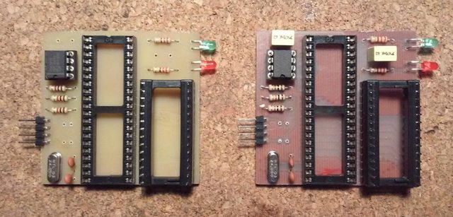
And here completed PCB with all components populated
Burning firmware
Having done that, I’ve started to burn firmware on AVRs – in this case, ATmega8515.
Here is a quick hack that I’ve created for this purpose
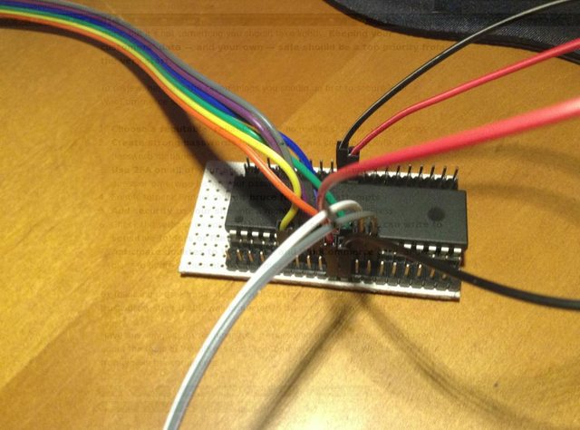
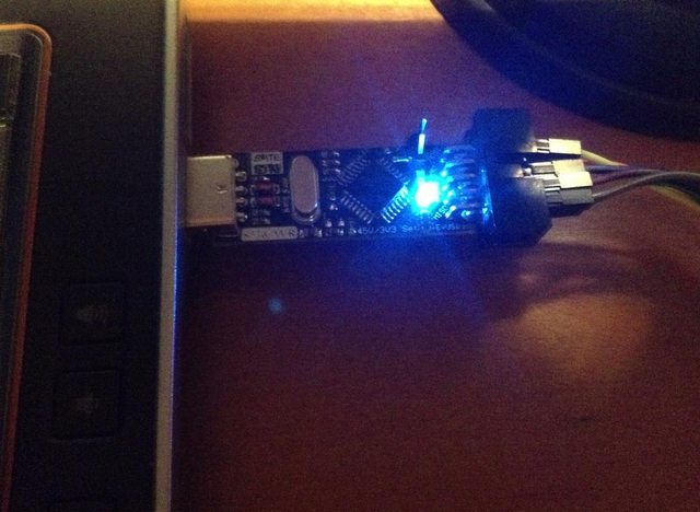
Programming is done via USBasp dongle
However, instead of the proper SID tune, I was getting squeaking sounds.
At first, I thought that I’ve burned the wrong fuse bits – nope.
Later, that may be the wrong components – nope again.
I’ve checked everything 10 times. Also, Swinkels suggested that squeaking might be caused by using the wrong DAC so I’ve ordered new DACs – TDA1543 (not TDA1543A) – still nope.
In the end, It turned out that I was using the wrong firmware file all the time…

But I finally got it working! YAY!
AVR implementation of C64 chip – SID from pit on Vimeo.
So yeah, that all worked fine and the project was really fun but that is not the end of the story yet :>
Going “PRO”
SwinSID SE is very nice but SwinSID NANO is nicer!
Unfortunately, NANO is a bit harder but still doable if you know some tricks.
Nicolas Welte of x1541.de did a great job and scaled down the original SwinSID project to a SID chip size. I’ve contacted Nicolas and he gave me a green light with using his board layout.
Thing is that this layout had to be machined with professional CNC tools.
I only have a small, homemade PCB router which is for prototyping purposes and has some limitations. (it will be covered in another post)
Sending projects to production requires modifications according to the manufacturer’s guidelines, so I had to apply a few changes.
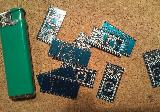
That wasn’t too hard and after several days, I received a package with nice and clean PCBs. Big thanks to Willy of Lamers for hints about PCB manufacturers.
ZOMG ! some soldering skillz needed
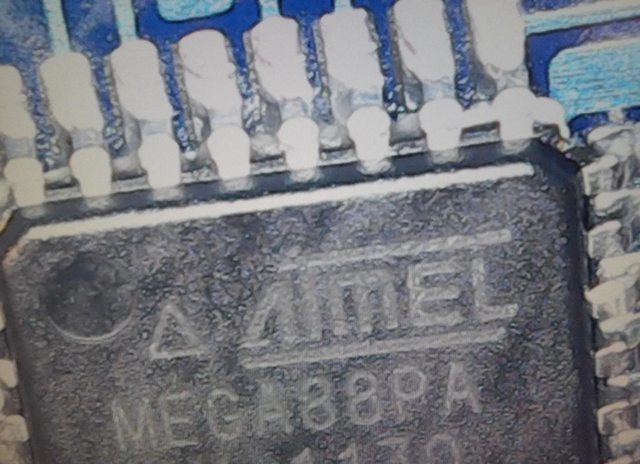
First things first, in this case, it means soldering the MEGA88PA chip on a PCB.
It might look hard to do with a simple soldering iron but in fact, it is quite easy if you have thin solder, good flux, soldering wick, and a steady hand 😉
Here are a few PCBs with chips already populated
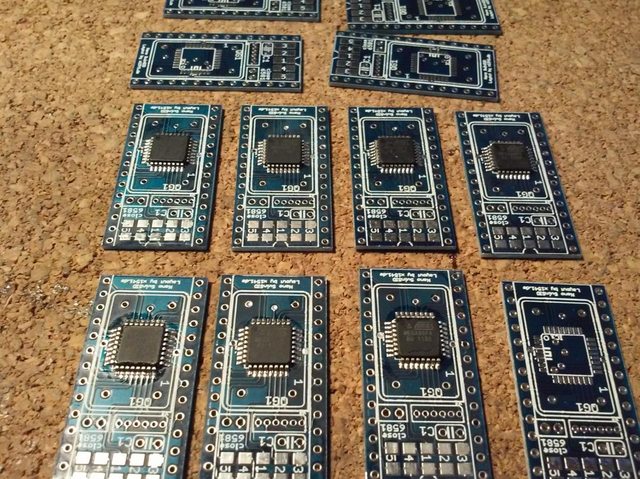
Using a cheap USB microscope turned out to be very helpful for doing the proper inspection afterward.
Firmware
This time, I’ve double-checked if I have the proper file 😀
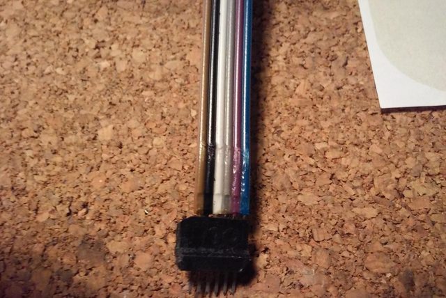
As you can see there are 6 small vias that are used to burn firmware to freshly soldered on MEGA88PA.
This actually required creating an awesome piece of engineering with a wicked name – The Connector.
It was made out of desoldered SATA port, a few wires, a bit of epoxy resin, some bee wings, and zombie poo.
It looks like this:
Let the burning begin!
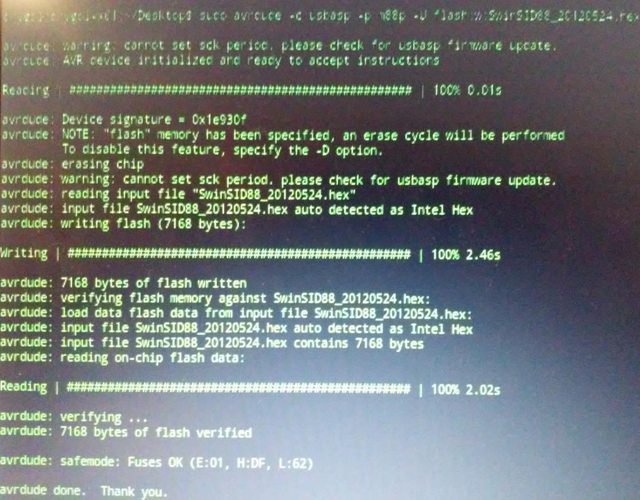
BOOM and it worked out of a box …. to my surprise
More soldering
Again, not so hard after all but I definitely do not recommend soldering it after a few heavy shots. Unfortunately, it turns on a specific video effect called – Motion Blur and it lasts till the next morning, so be careful ;>
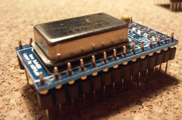
Components that have to be soldered on are simply five SMD resistors, one capacitor, pins, and a bulky clock generator which additionally serves as a radiator to the MEGA88 chip.
This is how it looks in its final form.
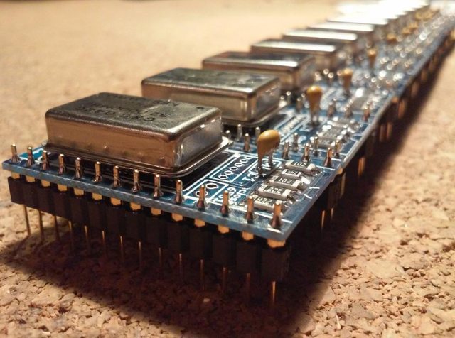
I’ve made quite a few of these and will be most probably selling them.
No worries, I’ll create a link to a store on my main page soon.

Testing
Finally here is how it works … and yeah enjoy this TekknoChipTune 😉
Nano SwinSID – Testing complete ;P from pit on Vimeo.
Cheers 😉
OUTRO
If you want to get retro gear or hardware modules, please visit our shop
New products are being added every month.
Also, please support our work by spreading info about it.
Without your support, we simply cannot grow and we have a lot of new cool retro hardware (and more) products to come 